The program software adopts the shell technology. Some popular anti-virus software may have false alarm issues. Please add trust. This module is an economical MODBUS-485 relay module with a dedicated integrated circuit as the core, which realizes the standard MODBUS-485 communication function. It can be used with 9V, 12V or 24V voltages. This module supports all common combinations of baud rates, stop bits and parity bits, and the MODBUS address can be set arbitrarily. These configurations are all set through the 485 communication port and can be reset to the default settings, that is, 9600 baud rate, 8 data bits, even parity, and 1 stop bit, through the buttons on the product.
This product is an economical MODBUS-RTU RS-485 relay module implemented with ASIC technology. The product may be powered from 5V, 9V, 12V, 18V, or 24V. This product supports all combinations of common baud rates, stop bits, and check bits, and its MODBUS-RTU address may be arbitrarily configured. These configurations are set through the RS-485 communication port, and through the button on the product, may be reset to the factory default, which is address 0x02, 9600 baud rate, 8 data bits, even parity, 1 stop bit. The functionality of the product is completely customizable in mass production as needed.
1.2 Structural Description
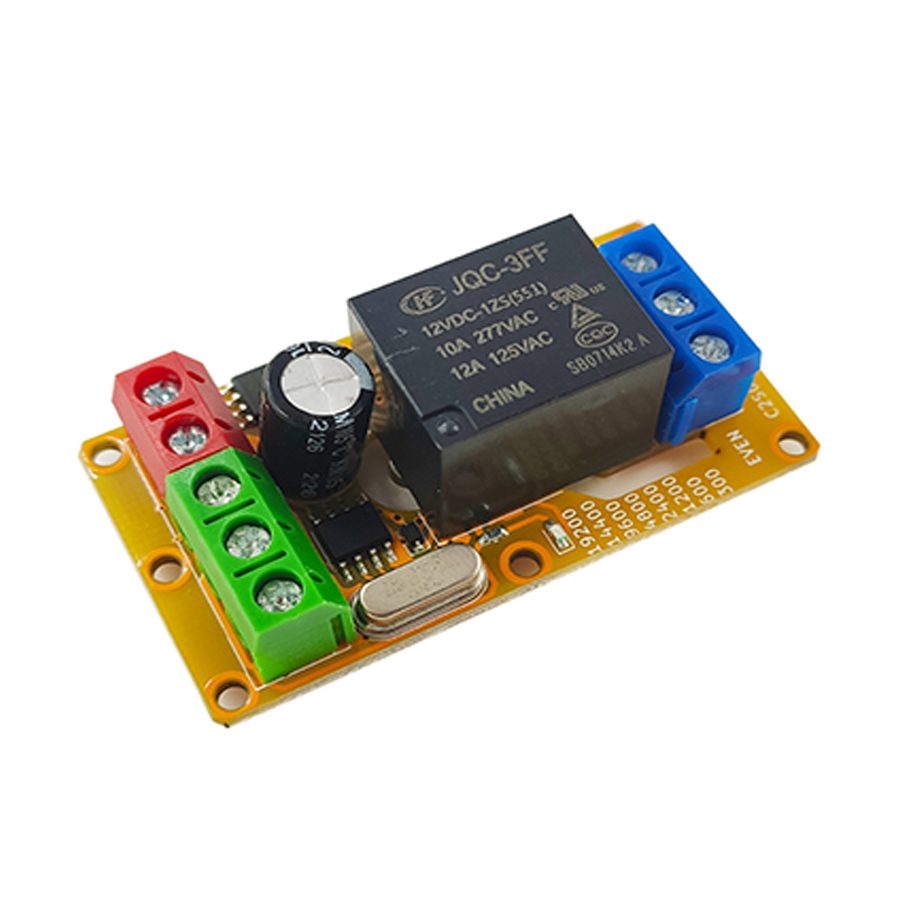
There are eight screw terminals, one button, and two LED indicators. The description of each terminal and component is shown in the table below. For B2J03, an extra white expansion header is present for the complimentary sensor analog input.
Name
No.
Meaning
Input terminal
0
Digital input with high sensitivity. Green. For B2J03, analog voltage readings are also available.
Differential positive
1
The positive terminal (A) of RS-485 communication differential twisted pair. Green.
Differential negative
2
The negative terminal (B) of RS-485 communication differential twisted pair. Green.
Normally open contact
3
The Normally Open (NO) contact of the relay. Blue. When the relay makes, this is connected to the common contact. For transistor output type, this serves as the load ground.
Common contact
4
The COMmon (COM) contact of the relay. Blue. For transistor output type products, this serves as the load-side power supply ground.
Normally closed contact
5
The Normally Closed (NC) contact of the relay, when the relay breaks, this is connected to the common contact. Blue. For transistor output type, this serves as the common terminal of load and load-side supply.
Positive supply
6
Positive power supply. The typical current consumption when the relay makes is 40 mA. Red.
Negative supply
7
Negative power supply. The typical current consumption when the relay makes is 40 mA. Red.
Reset button
8
The button for the reset module when powered up. Black.
The power supply terminals are directly connected to the DC power input. The normally open and normally closed relay terminals are connected according to the application needs, and they are connected in series with the load and load power supply. The digital input of the product is connected to an external voltage, and its 485 communication port is connected to the 485 bus according to the corresponding polarity. For the transistor output type, the wiring diagram is described in section 4.2. A typical wiring diagram of the relay output type is shown below.
When the product lacks a case, it is only recommended for controlling the safe voltage (0-36V) rather than the AC mains. Special care should be taken to prevent electric shock when a caseless product is used to control the AC mains. Please be gentle when tightening the screws to avoid stressing the product PCB. Long-term reliability of the product may be affected when the screw is too overtightened. When the product has a case, it can be used to control the AC mains. It can optionally be glued onto a flat surface with double-sided adhesive tape.
Chapter 2: Detailed Function Description
2.1 Introduction to MODBUS-RTU
This product provides a half-duplex RS-485 serial communication port. It uses two serial differential lines to transmit data: A (negative polarity) and B (positive polarity). As RS-485 adopts differential signaling, the transmission distance is considerably far, reaching the order of several kilometers; if a repeater is added, the communications reach even further. The two lines of RS-485 are responsible for both receiving and sending, so they are half-duplex, that is, receiving and sending cannot be performed at the same time. For all modules on the same RS-485 bus, their serial communication parameters are all the same.
To communicate between the master and the module, a communication protocol called MODBUS-RTU is required to regulate the data transmission between them. MODBUS is an industrial standard field bus proposed by MODICON, which has become one of the first choices for industrial control. It includes MODBUS-RTU and MODBUS-ASCII, and makes use of multiple physical media. Specifically, this module uses the MODBUS-RTU protocol based on the RS-485 physical layer.
The data transmission of MODBUS-RTU is carried out in "frames". A "frame" is an Application Data Unit (ADU). In the ADU, when the address code header and the CRC16 checksum tail are removed, the remaining part is a Protocol Data Unit (PDU). The maximum ADU length supported by this module is 9 bytes, and ADUs exceeding this length will be directly truncated.
In the serial-based MODBUS-RTU, the default communication format used is 1 start bit, 8 data bits, 1 even parity bit, and 1 stop bit. The data is in Big Endian (BE), that is, the higher bytes get transmitted first. The "address code" in ADU is an 8-bit value; in order to communicate with the module normally, this value should be consistent with the module's setting. 0x00 is a special address used for broadcasting. This module responds to this address but does not reply any data. The final checksum is a 16-bit CRC16 checksum, and its generating polynomial is 0xA001. It is worth noting that the transmission of the CRC16 value is in Little Endian (LE), that is, the low byte is in front and the high byte is in the back. The CRC16 performs a check on the entire ADU, including the PDU and the address field.
All MODBUS-RTU function codes supported by this module are listed in the following sections, and unlisted commands are not supported. This module supports the circumstances where the CRC16 is not required. When reliability is not mandatory and development efficiency is at a premium, the CRC16 may be replaced with 0000, and this module also responds to such commands.
2.1.1 Read Coils
To read the value of the coil, use the "Read Coil" command (function code 0x01). The start address of the coils (two bytes) and the number of coils to be read (two bytes) need to be specified when reading the coils.
MODBUS-RTU Read Coil Command (PDU)
Instruction Format
Normal Return Value Format
Error Return Value Format
0x01 (one byte) Start address A (two bytes) Number of coils N (two bytes)
0x01 (one byte) Number of bytes K (one byte) Coil data (one byte) Coil data (one byte) Coil data (one byte) ... (k-3 bytes)
0x81 (one byte) Exception code (one byte)
The maximum number of coils reads allowed by the MODBUS-RTU protocol itself is 0x07D0, while this module supports a maximum of 1. Therefore, the start address must be 0x0000, and the number of coils must be 0x0001.
Address
Name
Meaning
Power-up Default Value
0x0000
DOUT0
Digital output 0 coil value
0
In the normal return values, the coil data is packed into 8-bit bytes. The 8 lowest-address coils will be sent back first, followed by the 8 next lower address coils, and so on. In each byte, the highest bit corresponds to the highest-address coil. If the number of coils read back is not a multiple of 8, the missing high bits of the last byte will be filled with 0. If an error occurs during the execution of the instruction, an error message is returned.
In the example below, we assume that the slave address is 0xAA, and the master reads 11 coils from 0x0001-0x000B. Among these 11 coils, the odd address coils are all 1 (on), and the even address coils are all 0 (off).
MODBUS-RTU Read Coil Example (ADU)
Host Send Sequence
Slave Normal Return Value Sequence
Slave Error Return Sequence
0xAA 0x01 0x00 0x01 0x00 0x0B CRC16
0xAA 0x01 0x02 0x55 0x05 CRC16
0xAA 0x81 Exception code CRC16
2.1.2 Read Digital Inputs
To read the value of the digital input, use the "Read Digital Input" command (function code 0x02). The start address of the digital inputs (two bytes) and the number of digital inputs to be read (two bytes) need to be specified when reading the digital inputs.
MODBUS-RTU Read Digital Input Command (PDU)
Instruction Format
Normal Return Value Format
Error Return Value Format
0x02 (one byte) Start address A (two bytes) Number of input N (two bytes)
0x02 (one byte) Number of bytes K (one byte) Input data (one byte) Input data (one byte) Input data (one byte) ... (k-3 bytes)
0x82 (one byte) Exception code (one byte)
The maximum number of digital input reads allowed by the MODBUS-RTU protocol itself is 0x07D0, while this module supports a maximum of 1. Therefore, the start address must be 0x0000, and the number of digital inputs must be 0x0001.
Address
Name
Meaning
Power-up Default Value
0x0000
DIN0
Digital input 0 value
----
In the normal return values, the digital input data is packed into 8-bit bytes. The 8 lowest-address digital inputs will be sent back first, followed by the 8 next lower address digital inputs, and so on. In each byte, the highest bit corresponds to the highest-address digital input. If the number of digital inputs read back is not a multiple of 8, the missing high bits of the last byte will be filled with 0. If an error occurs during the execution of the instruction, an error message is returned.
In the example below, we assume that the slave address is 0xAA, and the master reads 13 input channels from 0x0000-0x000C. Among these 13 digital inputs, the odd address inputs are all 1 (high-level), and the even address inputs are all 0 (low-level).
MODBUS-RTU Read Digital Input Example (ADU)
Host Send Sequence
Slave Normal Return Value Sequence
Slave Error Return Sequence
0xAA 0x02 0x00 0x00 0x00 0x0D CRC16
0xAA 0x02 0x02 0xAA 0x0A CRC16
0xAA 0x82 Exception code CRC16
2.1.3 Read Holding Registers
To read the value of the holding registers, use the "Read Holding Register" command (function code 0x03). The start address of the holding registers (two bytes) and the number of holding registers to be read (two bytes) need to be specified when reading the holding registers.
MODBUS-RTU Read Holding Register Command (PDU)
Instruction Format
Normal Return Value Format
Error Return Value Format
0x03 (one byte) Start address A (two bytes) Number of register N (two bytes)
0x03 (one byte) Number of bytes K (one byte) Register 1 higher bits (one byte) Register 1 lower bits (one byte) Register 2 higher bits (one byte) ... (k-3 bytes)
0x83 (one byte) Exception code (one byte)
The maximum number of holding register reads allowed by the MODBUS-RTU protocol itself is 0x007D, while this module supports a maximum of 4. Therefore, the start address must not exceed 0x0003, and the number of registers plus the start address must not exceed 0x0004.
Address
Name
Meaning
Power-up Default Value
0x0000
NAME
Name register
Last configuration
0x0001
SRLCFG
Serial port configuration register
Last configuration
0x0002
LOCK
Lock register
0x0000
0x0003
DELAY
Jog delay register
0x0000
0x0004
PRTCFG
Protocol configuration register
Last configuration
0x0005
THRES
Level threshold register
Last configuration
0x0006
COUNT
Input counting register
0x0000
0x0007
FILTER
Input filtering register
Last configuration
0x0008
TRIG
Trigger delay register
Last configuration
0x0009
PWMCTL
PWM period register
0x0000
0x000A
PWMDTY
PWM duty register
0x0000
In the normal return value, the holding register data is returned in order. The lowest-address holding register will be sent back first, followed by the next lower address holding register, and so on. For each 16-bit value, the higher 8 bits are transmitted first, followed by the lower 8 bits. If an error occurs during the execution of the instruction, an error message is returned.
In the example below, we assume that the slave address is 0xAA, and the master reads 2 holding registers from 0x0000-0x0001. The value of the first register is 0x0BB8, and the value of the second register is 0x1B58.
MODBUS-RTU Read Holding Register Example (ADU)
Host Send Sequence
Slave Normal Return Value Sequence
Slave Error Return Sequence
0xAA 0x03 0x00 0x00 0x00 0x02 CRC16
0xAA 0x03 0x04 0x0B 0xB8 0x1B 0x58 CRC16
0xAA 0x83 Exception code CRC16
2.1.4 Read Input Registers
To read the value of the input registers, use the "Read Input Register" command (function code 0x04). The start address of the input registers (two bytes) and the number of input registers to be read (two bytes) need to be specified when reading the input registers.
MODBUS-RTU Read Input Register Command (PDU)
Instruction Format
Normal Return Value Format
Error Return Value Format
0x04 (one byte) Start address A (two bytes) Number of register N (two bytes)
0x04 (one byte) Number of bytes K (one byte) Register 1 higher bits (one byte) Register 1 lower bits (one byte) Register 2 higher bits (one byte) ... (k-3 bytes)
0x84 (one byte) Exception code (one byte)
The maximum number of holding register reads allowed by the MODBUS-RTU protocol itself is 0x007D, while this module supports a maximum of 2. Therefore, the start address must not exceed 0x0001, and the number of registers plus the start address must not exceed 0x0002.
Address
Name
Meaning
Power-up Default Value
0x0000
PRODID
Product ID
0x2301
0x0001
VERID
Version ID (The first 8 bits are the main version number, and the last 8 bits are the minor version number)
0x0020
0x0020
AIN0
Analog input 0
----
0x0021
AIN1
Analog input 1
----
In the normal return value, the returned input data is returned in order. The lowest-address input register will be sent back first, followed by the next lower address input register, and so on. For each 16-bit value, the higher 8 bits are transmitted first, followed by the lower 8 bits. If an error occurs during the execution of the instruction, an error message is returned.
In the example below, we assume that the slave address is 0xAA, and the master reads 2 registers from 0x0000-0x0001. The value of the first register is 0x0BB8, and the value of the second register is 0x1B58.
MODBUS-RTU Read Input Register Example (ADU)
Host Send Sequence
Slave Normal Return Value Sequence
Slave Error Return Sequence
0xAA 0x04 0x00 0x00 0x00 0x02 CRC16
0xAA 0x04 0x04 0x0B 0xB8 0x1B 0x58 CRC16
0xAA 0x84 Exception code CRC16
2.1.5 Write Single Coil
To change the value of a single coil, use the "Write Single Coil" command (function code 0x05). The state constant in the request data field indicates the requested coil state: 0xFF00 requests the coil to turn on, and 0x0000 requests the coil to turn off. All other values are illegal and have no effect on the output. For the description of the coil of this machine, please refer to the "Read Coils" section.
MODBUS-RTU Write Single Coil Command (PDU)
Instruction Format
Normal Return Value Format
Error Return Value Format
0x05 (one byte) Coil address A (two bytes) State constant (two bytes)
0x05 (one byte) Coil address A (two bytes) State constant (two bytes)
0x85 (one byte) Exception code (one byte)
In the normal return value, the coil address and status constant will be echoed. For each value, the higher 8 bits are transmitted first, followed by the lower 8 bits. If an error occurs during the execution of the instruction, an error message is returned.
In the example below, assume that the slave address is 0xAA, and the master turns on the coil at address 0x000B.
MODBUS-RTU Write Single Coil Example (ADU)
Host Send Sequence
Slave Normal Return Value Sequence
Slave Error Return Sequence
0xAA 0x05 0x00 0x0B 0xFF 0x00 CRC16
0xAA 0x05 0x00 0x0B 0xFF 0x00 CRC16
0xAA 0x85 Exception code CRC16
2.1.6 Write Single Holding Register
To write the value of a single holding register, use the "Write Single Holding Register" command (function code 0x06). The start address of the holding registers (two bytes) and the value of holding registers to be written (two bytes) need to be specified when writing the holding registers. For the description of the holding registers of this machine, please refer to the section "Read Holding Registers".
MODBUS-RTU Write Single Holding Register Command (PDU)
In the normal return value, the register address and register value will be echoed. For the register value, the upper 8 bits are transmitted first, followed by the lower 8 bits. If an error occurs during the execution of the instruction, an error message is returned.
In the example below, we assume that the slave address is 0xAA, and the master writes 0x0BB8 into the holding register at address 0x0001.
MODBUS-RTU Write Single Holding Register Example (ADU)
Host Send Sequence
Slave Normal Return Value Sequence
Slave Error Return Sequence
0xAA 0x06 0x00 0x01 0x0B 0xB8 CRC16
0xAA 0x06 0x00 0x01 0x0B 0xB8 CRC16
0xAA 0x86 Exception code CRC16
2.1.7 Possible Exception Codes
There is an exception code field in the error return value of MODBUS-RTU. The user can judge the problem that the device cannot execute the instruction correctly through the exception code. The four exception codes used in this machine are listed in the table below.
Exception Codes
Name
Meaning
0x01
ENOFUNC
This device does not support this function code, if the function code sent is not listed in this chapter.
0x02
ENOADR
The requested element addresses include ones that are not available in this device, such as coil address and number out of range.
0x03
EINVAL
The length of the command does not comply with the specifications, or some necessary fields are missing in the command.
0x04
EDEVICE
The device encountered an error while executing commands, such as writing invalid values to holding registers or other unexpected failures.
2.2 Serial Port Configuration Description
This product encompasses many combinations of baud rate, parity bit, and stop bit. These combinations are set through the serial port configuration holding register SRLCFG (address 0x0001). To protect SRLCFG from unintended modifications, a lock holding register LOCK (address 0x0002) is implemented to unlock the write to SRLCFG. A name holding register NAME (address 0x0000) is also implemented to facilitate users' identification of module instances, and writes to it also require the LOCK register to be unlocked. If a change to the name or configuration of the module is proposed, ASCII code "UL" (i.e., 0x554C) must be written to the lock holding register LOCK before writing NAME or SRLCFG. All writes to registers are effective immediately. For this particular module, only "Read Holding Register" (function code 0x03) and "Write Single Holding Register" commands (function code 0x06) are recognized for reading and writing these registers. The "Write Multiple Holding Registers" command (function code 0x10) is not supported.
To reset the module name and serial port configuration to factory default, all circuit connections to the module must be removed first. Keep the button pressed, then connect the power supply to the module. Release the reset button after 5 seconds and power cycle the module. The module then returns to the default settings of name ASCII code "UD" (i.e., 0x5544), address 0x02, 9600 baud rate, 8 data bits, 1 even parity bit, 1 stop bit. Further reconfiguration of the module may begin here.
It is certainly possible to use dedicated software to configure these parameters. When doing so, connect the module to the computer through a USB to RS-485 cable and specify the serial port number on the computer; the module may then be easily configured.
2.2.1 Lock Holding Register
The address of the lock holding register LOCK is 0x0002. To unlock the module configuration protection, please use the "Write Single Holding Register" command (function code 0x06) to write 0x554C to this address; writing any other value has no effect, and the value of the register will remain locked with a value of 0x0000. To check whether the unlocking is successful, use the "Read Holding Register" command (function code 0x03) to read LOCK and see if the value is 0x554C. After the register is successfully unlocked, the module will relock this register if it detects any instruction that targets other modules, instructions with parity errors, or instructions with wrong CRC16 on the bus. Reading this register will not cause re-locking. Writing to NAME and SRLCFG will cause relocking regardless of whether the write is successful or not.
2.2.2 Name Holding Register
The address of the name holding register NAME is 0x0000. This register is implemented to facilitate users' queries and module identification. To write to this register, the lock holding register LOCK needs to be unlocked. After unlocking, writing to this register will change the module name and relock the configuration lock.
2.2.3 Serial Port Configuration Holding Register
The address of the serial port configuration holding register SRLCFG is 0x0001. To write to this register, you need to unlock it as described in the previous section. After unlocking, writing to this register will configure the module parameters and relock the configuration lock. If an incorrect configuration is written to the register, the configuration will be rejected, the original configuration will remain unchanged, and the configuration lock will be relocked. The factory default configuration is 9600 baud rate, even parity, 1 stop bit, and MODBUS address 0x02.
Bit Segment
Meaning
Value
[15:14]
Number of stop bits in the serial port
11: Reserve, do not use 10: 2 stop bits 01: 1.5 stop bits 00: 1 stop bit
[13:12]
Parity check of the serial port
11: Reserve, do not use 10: Even parity 01: Odd parity 00: No parity
Relay type: DC 30V or AC 0 - 220V, 8A Transistor type: DC 12 - 48V, 8A
Output isolated voltage
Relay type: Less than 250V Transistor type: Less than 130V
Operating temperature
-20 - 60℃
5.2 Absolute Maximum Ratings
The extreme conditions that this module can withstand are shown in the following table. Stresses at or above those listed here may permanently damage the module.
Description
Range
Supply voltage
5V DC: 5.3V 9V DC: 11.5V 12V DC: 15V 24V DC: 30V
Self-resettable fuse
DC 30V, 500mA
Communication stress
DC 50V
Input stress
DC 50V
Output stress
Relay type: AC 250V, 10A Transistor type: DC 55V, 10A
Output isolating voltage
Relay type: DC 1000V, 60s (Type test only) Transistor type: DC 250V, 60s (Type test only)
Relay mechanical life
Relay type: More than 100,000 times (Actual life varies with load, > 10,000 times under heavy load)
Storage temperature
-40 - 85℃
5.3 Other Parameters and Certifications
The other parameters and certifications of this module are listed as follows. These parameters and certifications include electrostatic discharge, electrical fast transient, and voltage surge tests that comply with the requirements of IEC61000-6-1-2016 (Edition 3.0, 2016-08) for light industry purposes. During all of these tests, the modules are powered by a well-grounded 12V supply and in active delay operation.
Item
Details
Passing Criterion
Electrostatic discharge resistance
IEC61000-4-2: 1kV, discharge on all terminals.
(A) Module functions normally.
Electrostatic discharge resistance
IEC61000-4-2: 2kV, discharge on all terminals.
(C) Module is not permanently damaged.
Electrical fast transient resistance
IEC61000-4-4: 500V, 5kHz, 2min, applied to all terminals.
(A) Module functions normally.
Electrical fast transient resistance
IEC61000-4-4: 1kV, 5kHz, 2min, applied to all terminals.
(C) Module is not permanently damaged.
Surge resistance
IEC61000-4-5: 1kV voltage surge to ground, applied to power terminals. (Guaranteed by design)
(C) Module is not permanently damaged.
Creepage distance
IEC60950-2L/2N: Pollution degree 3, material category IIIa and IIIb, basic isolation from relay terminal to logic side, creepage distance above 6mm.
The actual distance is above 9.2mm, which meets the requirements.
Electrical clearance
IEC60950-2H: Pollution degree 3, basic isolation from relay terminal to logic side, electrical clearance above 2mm.
The actual distance is above 2.2mm, which meets the requirements.
5.4 Notes on Reliability
This module is only qualified for commercial applications due to its miniature size, thus it is not recommended for formal industry situations with strong interference. Additional power filters and/or port filters are required if it must be used in this way. If such additional filters are not desired, a switching power supply with Electrical Fast Transient (EFT) resistance is required to power the module, and the power supply cord must be shorter than 3m.
In addition, if the load exhibits current spikes during startup or emits extremely strong EMI during operation, it is recommended to use standalone power sources for the module and to place these loads as far as possible from the module, or the module may repeatedly reset when the load powers on, especially in cases where the power source has poor transient responsiveness or the 5V version is used.
During the test, the negative supply of the module is directly connected to the earth by default. The same connection should be made to obtain the stability index in the table above.
Chapter 6: Appendix
6.1 Typical Application
A temporary LED lighting spotlight on a construction site needs to be remotely and automatically controlled by a computer. At the same time, there must be a switch beside the light, through which the light may be manually controlled. The LED spotlight is powered by a 12V battery.
6.1.1 Requirement Analysis
In this application, one input and one relay output are used, and the module connects to the computer through an RS-485 interface. The system is powered by a 12V supply and may be fulfilled with a module of model B2J031M31. Since there may be other modules mounted on the MODBUS-RTU bus, a unique communication address needs to be designated for this module. We assume that the address is 0x23. We also assume that the bus has a baud rate of 19200 and uses odd parity with 2 stop bits.
Frequently Asked Questions
What protocol and bus does the B2J03 relay module use?
The B2J03 is a single-channel MODBUS-RTU slave on a half-duplex RS-485 bus. It uses two differential lines, A (negative) and B (positive), so distances of several kilometres are achievable, further with a repeater. It supports standard function codes 0x01-0x06 (read coils, read inputs, read holding/input registers, write single coil, write single register).
What supply voltages and output ratings does the B2J03 support?
The module accepts 5V, 9V, 12V, 18V, or 24V DC supply with current consumption under 50 mA. Relay-output types switch DC 30V or AC 0-220V at 8A; transistor-output types switch DC 12-48V at 8A. The relay offers NO, NC, and COM contacts with a mechanical life above 100,000 operations.
How do I set the MODBUS address, baud rate, and parity on the B2J03?
Serial parameters live in the SRLCFG holding register (0x0001). First unlock by writing 0x554C to the LOCK register (0x0002), then write SRLCFG. You can set address 0x01-0xF7, baud rates 300-28800, odd/even/no parity, and 1/1.5/2 stop bits. All writes take effect immediately and relock the configuration afterward.
How do I reset the B2J03 to factory defaults?
Remove all circuit connections, hold the reset button, then apply power. Release the button after 5 seconds and power-cycle the module. It returns to its defaults: name "UD", address 0x02, 9600 baud rate, 8 data bits, even parity, and 1 stop bit. Reconfiguration through the RS-485 port can then begin.
Is the B2J03 suitable for harsh industrial environments?
It is an economical, miniature module qualified for commercial use; it passes ESD, electrical fast transient, and surge tests per IEC 61000-6-1. For strong-interference industrial sites, add power/port filters or use an EFT-resistant switching supply with a power cord under 3 m. Operating temperature is -20 to 60 degrees C.